End-point view requested in your document: module and block-level hardware design code with clear
definitions beside each module.
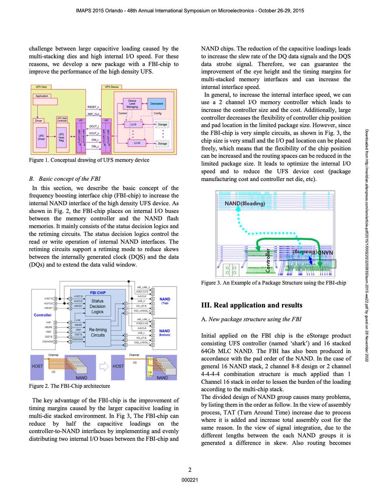
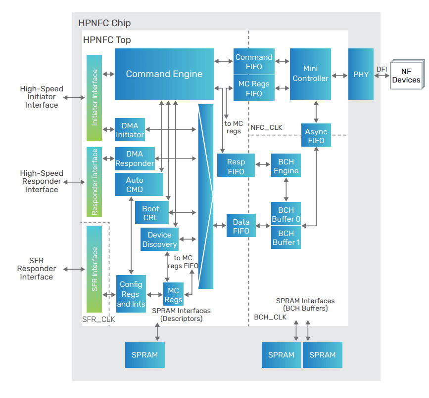
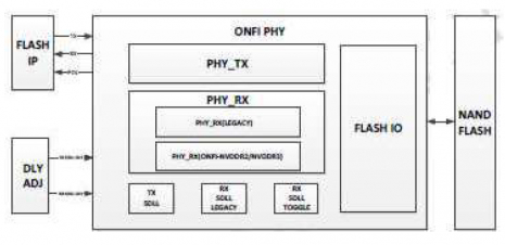
Module A: NPHY Command FIFO Path
module nphy_cmd_path (
  input  logic        clk,
  input  logic        rst_n,
  input  logic [63:0] host_cmd,
  input  logic        host_cmd_v,
  output logic        host_cmd_r,
  output logic [63:0] phy_cmd,
  output logic        phy_cmd_v,
  input  logic        phy_cmd_r
);
  logic [63:0] cmd_fifo_dout;
  logic        cmd_fifo_empty;

  async_fifo #(.WIDTH(64), .DEPTH(16)) u_cmd_fifo (
    .wclk(clk), .wrst_n(rst_n), .wvalid(host_cmd_v), .wready(host_cmd_r), .wdata(host_cmd),
    .rclk(clk), .rrst_n(rst_n), .rvalid(!cmd_fifo_empty), .rready(phy_cmd_r), .rdata(cmd_fifo_dout)
  );

  assign phy_cmd   = cmd_fifo_dout;
  assign phy_cmd_v = !cmd_fifo_empty;
endmodule
Definition: Buffers and forwards host/controller command traffic into the NPHY-facing
command stream using FIFO-safe flow control.
Module B: FBI Retiming Controller
module fbi_retimer_ctrl (
  input  logic       clk,
  input  logic       rst_n,
  input  logic [7:0] skew_metric,
  input  logic       training_req,
  output logic [2:0] dq_delay_sel,
  output logic       retrain_done
);
  typedef enum logic [1:0] {IDLE, TRAIN, LOCK} state_t;
  state_t state;

  always_ff @(posedge clk or negedge rst_n) begin
    if (!rst_n) begin
      state <= IDLE;
      dq_delay_sel <= 3'd0;
      retrain_done <= 1'b0;
    end else begin
      case (state)
        IDLE:  if (training_req) state <= TRAIN;
        TRAIN: begin
          dq_delay_sel <= skew_metric[7:5];
          state <= LOCK;
        end
        LOCK: begin
          retrain_done <= 1'b1;
          if (training_req) state <= TRAIN;
        end
      endcase
    end
  end
endmodule
Definition: Digital FBI control FSM for selecting retiming delay based on measured
skew/timing status.
Module C: DMA + ECC Data Plane
module nand_data_plane (
  input  logic         clk,
  input  logic         rst_n,
  input  logic [255:0] dma_in_data,
  input  logic         dma_in_v,
  output logic         dma_in_r,
  output logic [255:0] nand_wr_data,
  output logic         nand_wr_v,
  input  logic         nand_wr_r
);
  logic [255:0] ecc_data;
  logic         ecc_v;

  bch_encode u_bch (
    .clk(clk), .rst_n(rst_n),
    .in_data(dma_in_data), .in_valid(dma_in_v), .in_ready(dma_in_r),
    .out_data(ecc_data), .out_valid(ecc_v), .out_ready(nand_wr_r)
  );

  assign nand_wr_data = ecc_data;
  assign nand_wr_v    = ecc_v;
endmodule
Definition: A digital path combining DMA payload movement and ECC preparation before
data reaches NAND write pipelines.